


The world of semiconductors is evolving rapidly, and Advanced Packaging Technologies are playing a pivotal role in the next generation of high-performance devices. Traditional packaging methods, which often focused on simply enclosing chips for protection, are giving way to more sophisticated techniques that improve performance, efficiency, and miniaturization. Two of the most promising technologies in this field—3D stacking and chiplet architectures—are enabling more compact and powerful semiconductor solutions that can meet the demands of modern applications such as artificial intelligence, edge computing, and the Internet of Things (IoT).
The Need for Advanced Packaging:
As the demand for smaller, faster, and more efficient electronic devices continues to grow, traditional semiconductor packaging faces several challenges:
Power and Performance: Semiconductor chips need to handle increasing workloads while minimizing power consumption. New packaging techniques are helping to optimize both aspects.
Miniaturization: With the miniaturization of consumer electronics, there’s a growing need for packaging solutions that can fit more functionality into smaller spaces.
Thermal Management: As semiconductors become more powerful, heat dissipation has become a critical factor. Advanced packaging helps address this by offering better thermal management solutions.
Cost-Effectiveness: Reducing costs while maintaining performance and size is a continuous challenge in semiconductor manufacturing, and packaging technology is helping meet this need by enabling more efficient production processes.
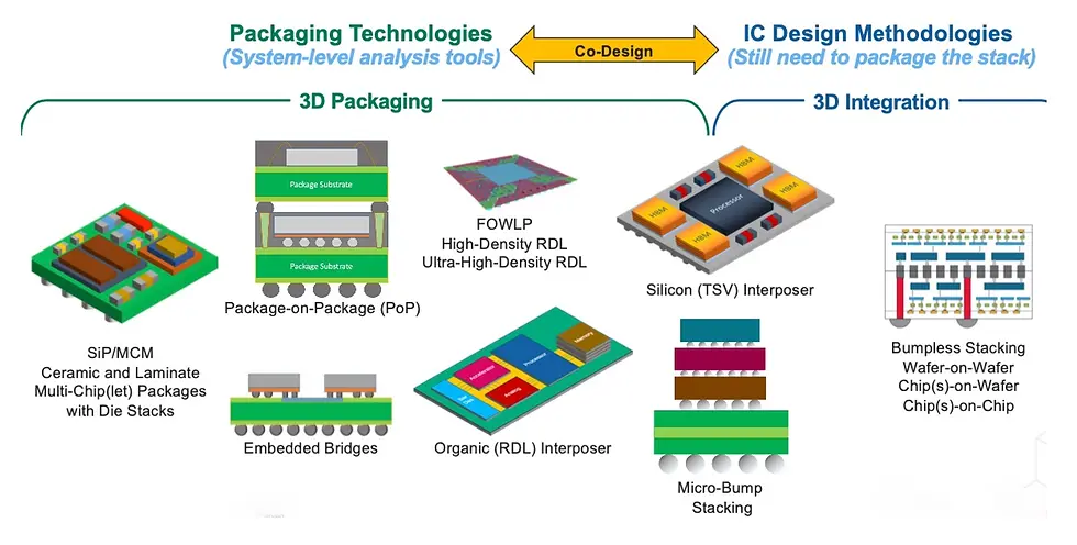
Key Advanced Packaging Techniques:
3D Stacking:
3D stacking involves vertically stacking multiple semiconductor layers or chips to create more compact, efficient, and powerful systems. This technique reduces the footprint of the device, making it ideal for use in mobile devices, wearables, and high-performance computing systems.
In a 3D stacked architecture, the chips are connected using through-silicon vias (TSVs) or microbumps, which allow for high-speed data transfer between layers. This leads to faster processing speeds and greater overall system performance without increasing the size of the device.
One of the most significant advantages of 3D stacking is that it enables more parallel processing, which is essential for applications like artificial intelligence and machine learning, where large data sets must be processed quickly.
Chiplet Architectures:
Chiplet-based packaging takes a modular approach to semiconductor design by breaking down the functions of a chip into smaller, discrete components called chiplets. Each chiplet can be optimized for specific tasks, allowing for greater flexibility, improved performance, and lower costs.
Chiplet architectures enable designers to mix and match different semiconductor components based on performance needs, without redesigning the entire chip. This allows for more customizable solutions and can significantly reduce time-to-market.
One key advantage of chiplet-based packaging is that it allows for the integration of multiple technologies on a single package. For example, a chiplet-based solution could integrate high-performance processing units with memory, power management, and other functions, all within the same device.
This modular approach also improves yield rates and manufacturing efficiency, as individual chiplets can be tested and manufactured separately before being assembled into the final package.
System-in-Package (SiP):
System-in-package (SiP) technology involves integrating multiple semiconductor devices—such as processors, memory, sensors, and power management circuits—into a single, compact package.
SiP solutions are increasingly being used in consumer electronics, medical devices, and IoT products, where small form factors and low power consumption are essential. The technology also allows for higher levels of integration, reducing the need for multiple packages and interconnects.
Fan-Out Wafer-Level Packaging (FOWLP):
Fan-Out Wafer-Level Packaging is a newer method that provides a high-density interconnect between the semiconductor chip and the external world. It offers improved electrical performance, better thermal dissipation, and a smaller form factor compared to traditional packaging methods.
FOWLP allows for a large number of I/O connections in a small package, making it ideal for applications in high-performance computing, mobile devices, and 5G technology.
Thermal Management Solutions:
With the increasing complexity and power requirements of modern semiconductor devices, thermal management has become a crucial aspect of packaging. Advanced packaging technologies such as heat spreaders, thermal vias, and microfluidic cooling systems are being developed to ensure that heat is efficiently dissipated from the chip.
These solutions help maintain performance levels and prevent overheating, which is particularly important in high-performance computing systems, AI accelerators, and data centers.
Advantages of Advanced Packaging:
Improved Performance:
By using 3D stacking and chiplet architectures, devices can achieve faster speeds and greater processing power without increasing their physical size. These packaging technologies enable shorter interconnects, reducing latency and improving overall system performance.
Lower Power Consumption:
Advanced packaging techniques allow for more efficient power usage. By improving thermal management and minimizing power loss in interconnects, these technologies help extend battery life in mobile devices and reduce the energy consumption of large-scale computing systems.
Cost Efficiency:
The use of modular chiplets and SiP solutions can reduce manufacturing costs by enabling the reuse of existing components and optimizing the supply chain. This leads to lower production costs, faster time-to-market, and the ability to scale production more easily.
Smaller Form Factor:
3D stacking and chiplet-based solutions allow for the development of more compact devices. With smaller, lighter electronics, consumers can enjoy high-performance products in increasingly portable and convenient form factors.
Flexibility and Customization:
Chiplet architectures enable more flexibility in design, allowing manufacturers to create custom solutions for specific applications, such as high-performance computing or IoT devices, without the need for a complete redesign of the chip.

Conclusion:
Advanced Packaging Technologies like 3D stacking and chiplet architectures are revolutionizing the semiconductor industry by enabling the creation of more powerful, efficient, and compact solutions. As the demand for faster, smaller, and more energy-efficient devices continues to rise, these innovations are playing a critical role in meeting the challenges of modern electronics. From improved performance to cost efficiency and customization, advanced packaging is driving the next generation of semiconductor products, positioning companies to stay competitive in an increasingly complex market.
As semiconductor manufacturers continue to push the boundaries of packaging, we can expect even more breakthroughs in performance, miniaturization, and integration, leading to smarter, more capable devices across industries.
Comentários